India has tried to build a semiconductor industry before. This is not a new aspiration. The first attempt dates to the 1980s, when a semiconductor fabrication facility was established at Chandigarh under the Semi-Conductor Laboratory (SCL). That facility suffered a devastating fire in 1989 that destroyed critical equipment, and while it was rebuilt, it never achieved the scale, technology level, or commercial viability needed to anchor a domestic semiconductor ecosystem. In the decades that followed, India watched as Taiwan, South Korea, China, and even smaller economies like Israel and Singapore built globally competitive semiconductor industries while India's chip fabrication capability remained stuck at technology nodes two to three generations behind the global frontier. The India Semiconductor Mission 2.0 (ISM 2.0), announced with a combined government and private sector investment exceeding $15 billion, represents India's most serious, most heavily capitalized, and most strategically urgent attempt to break this pattern. Whether it succeeds—and what "success" even means in this context—is one of the most consequential industrial policy questions facing the Indian economy.
Understanding why semiconductors matter requires understanding how comprehensively they have infiltrated every aspect of modern technology, economy, and national security. A modern smartphone contains approximately 15 billion transistors. A high-end data centre GPU (like NVIDIA's H100, which powers the AI revolution) contains 80 billion transistors. An advanced automobile contains over 3,000 individual semiconductor chips controlling everything from engine management to safety systems to infotainment. India imports virtually 100% of its semiconductor requirements—approximately $35-40 billion worth annually—making semiconductors India's third-largest import category after crude oil and gold. This import dependence creates a strategic vulnerability of extraordinary severity: during the 2020-2022 global chip shortage, Indian automobile manufacturers lost an estimated $8-10 billion in revenue because they simply could not obtain the chips needed to build cars. Factories sat idle. Completed vehicles sat on assembly lines missing a single $2 chip that controlled their brake lights. An entire industrial economy was held hostage by its dependence on a component manufactured 5,000 kilometers away in a Taiwanese clean room.
What ISM 2.0 Actually Proposes: The Four Pillars

The India Semiconductor Mission 2.0 is structured around four distinct investment pillars, each addressing a different segment of the semiconductor value chain. Understanding these pillars—and the critical distinctions between them—is essential to evaluating whether the mission is likely to achieve its objectives.
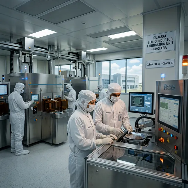
Semiconductor Fabrication (Fab): The flagship investment is in semiconductor fabrication plants—the enormously expensive, extraordinarily complex manufacturing facilities where silicon wafers are processed into finished chips through hundreds of sequential chemical, photolithographic, and etching steps. The Tata Electronics semiconductor fab at Dholera, Gujarat—a joint venture with Taiwan's Powerchip Semiconductor Manufacturing Corporation (PSMC)—is the mission's centerpiece project, with an estimated investment of $11 billion. This fab will manufacture chips at the 28-nanometer technology node, with planned upgrades to 12-nanometer capability. The 28nm node is not the most advanced technology available globally—TSMC's cutting-edge fabs produce chips at 3nm—but it is the "sweet spot" where the largest volume of global chip demand exists. Approximately 30-40% of all semiconductors manufactured worldwide are produced at 28nm or larger nodes, serving automotive, industrial, IoT, consumer electronics, and telecommunications applications. The strategic choice to start at 28nm rather than attempting frontier manufacturing is pragmatically sound: it targets the largest market segment, uses well-proven manufacturing technology, and avoids the extreme technical and financial risks of competing at the bleeding edge against TSMC and Samsung.
OSAT (Outsourced Semiconductor Assembly and Testing): Before a finished chip reaches a device manufacturer, the bare silicon die must be packaged—encased in a protective housing with electrical connections (pins, ball grid arrays) that allow it to be soldered onto a circuit board—and tested to verify that every one of its billions of transistors functions correctly. This assembly, packaging, and testing process (collectively called OSAT) is a distinct industry segment with different capital requirements and technical challenges than fabrication. India has attracted significant OSAT investment: Tata Electronics is building an OSAT facility in Assam, Micron Technology (the American memory chip manufacturer) is investing $2.75 billion in an assembly and test facility in Gujarat, and several other companies have announced OSAT projects. OSAT facilities require substantially lower investment than fabs ($1-3 billion versus $10-20 billion), achieve operational viability faster, and provide India's semiconductor workforce with hands-on industry experience that creates a talent pipeline for the more demanding fab operations.
Semiconductor Design: India's strongest existing position in the semiconductor value chain is in chip design—the process of creating the circuit architectures, logic designs, and physical layouts that define a chip's functionality before it is manufactured. India already employs approximately 125,000 semiconductor design engineers—roughly 20% of the global semiconductor design workforce—working for companies including Qualcomm, Intel, AMD, Texas Instruments, Broadcom, MediaTek, and Samsung. These engineers, based primarily in Bangalore, Hyderabad, and Noida, design chips that are manufactured in Taiwan, South Korea, and China—generating enormous intellectual value in India while the manufacturing value accrues elsewhere. ISM 2.0 aims to expand this design ecosystem by supporting domestic fabless chip design companies (companies that design chips but outsource manufacturing to foundries) through financial incentives, incubation support, and design infrastructure subsidies. The aspiration is for India to develop globally competitive chip design companies analogous to America's Qualcomm, NVIDIA, or AMD—companies that capture the highest-value segment of the semiconductor value chain without bearing the enormous capital burden of owning fabrication facilities.
Compound Semiconductors and Display Manufacturing: Beyond traditional silicon-based chips, ISM 2.0 includes investment in compound semiconductor manufacturing (gallium nitride, silicon carbide) and display panel fabrication. Compound semiconductors—which use materials other than pure silicon—are critical for specific high-performance applications: electric vehicle power electronics (silicon carbide MOSFETs and IGBTs enable faster switching and lower energy losses), 5G telecommunications infrastructure (gallium nitride amplifiers provide superior high-frequency performance), and renewable energy systems (SiC-based inverters improve solar panel efficiency). Display manufacturing—specifically OLED and advanced LCD panel production—addresses India's massive display import dependence for smartphones, televisions, and laptops.
What's Different This Time: Why ISM 2.0 Might Succeed Where Previous Attempts Failed
India's semiconductor pessimists—and there are many, with historically justified skepticism—point to the country's track record of ambitious industrial policy announcements that underdelivered. The Chandigarh SCL story, the repeatedly postponed fab projects of the 2000s and 2010s, the bureaucratic delays that caused multiple international semiconductor companies to abandon proposed Indian investments—these precedents create a legitimate credibility deficit. Here is why ISM 2.0 is structurally different from previous attempts:
The Geopolitical Window: The global semiconductor industry is undergoing a once-in-a-generation geographic restructuring driven by geopolitical risk. The concentration of advanced chip manufacturing in Taiwan—TSMC alone manufactures over 60% of the world's semiconductors and over 90% of the most advanced chips—creates a single point of failure that governments worldwide have belatedly recognized as an unacceptable strategic vulnerability. A Chinese military action against Taiwan would instantly disrupt the global technology economy. The United States has responded with the CHIPS Act ($52 billion in fab subsidies). The European Union has the European Chips Act (€43 billion). Japan has attracted TSMC to build a fab in Kumamoto. This global scramble to diversify semiconductor manufacturing away from Taiwan has created a geopolitical window where major semiconductor companies—TSMC, Samsung, Intel, Micron—are actively seeking new manufacturing locations, and governments worldwide are competing with subsidies to attract them. India's ISM 2.0 enters this window with competitive advantages (large domestic market, lower construction and labour costs, English-speaking engineering workforce) that did not align with industry incentives in previous decades.
Credible Industrial Partners: Previous Indian semiconductor initiatives were largely government-led, with limited engagement from established global semiconductor companies. ISM 2.0 features committed investments from credible industry players: Tata Electronics (backed by India's largest industrial conglomerate), Micron Technology (one of the world's three major memory chip manufacturers), PSMC (a Taiwanese foundry with proven manufacturing expertise), and Tower Semiconductor (an Israeli specialty foundry). These are not memoranda of understanding or letters of intent—they are executed investment agreements with construction timelines, equipment procurement contracts, and hiring plans. When Micron commits $2.75 billion to build an assembly and test facility in India, it is deploying capital based on a calculated business decision, not a political gesture.
The Domestic Market Anchor: India is the world's second-largest smartphone market (consuming over 150 million smartphones annually), the fastest-growing automobile market, a massive consumer of telecommunications equipment (deploying one of the world's largest 5G networks), and an increasingly significant data centre market. This domestic consumption creates a large, proximate market for domestically manufactured semiconductors—reducing logistics costs, simplifying supply chain management, and providing a guaranteed demand baseline that purely export-oriented fab investments in smaller countries cannot replicate.
The Honest Challenges: What Could Still Go Wrong
Water and Power Requirements: A semiconductor fab consumes staggering quantities of ultrapure water (approximately 30-40 million litres per day for a large facility) and electricity (a modern fab's power consumption is comparable to a small city). India's water stress—particularly in the western and southern regions where most industrial development occurs—and its electricity supply reliability (improving but still inconsistent in many areas) create genuine infrastructure risks. The Dholera fab's location was partly selected for its access to Narmada canal water, but ensuring uninterrupted, ultrapure water supply at the volumes required will be a continuous operational challenge.
Talent Development Timeline: India has semiconductor design engineers. What it lacks are semiconductor process engineers—the specialists who understand the physics and chemistry of semiconductor manufacturing: photolithography, chemical vapour deposition, ion implantation, chemical-mechanical planarization. Training a process engineer to the proficiency required for fab operations takes 3-5 years of supervised hands-on experience. India is starting this training pipeline essentially from zero. The partnerships with PSMC and Micron include technology transfer and training components, but building a domestically sufficient process engineering workforce is a decade-long endeavour.
Frequently Asked Questions (FAQs)
Why can't India just start manufacturing at 3nm like TSMC, instead of beginning at 28nm?
Manufacturing semiconductor chips at 3nm requires extreme ultraviolet (EUV) lithography machines—equipment manufactured by a single company on Earth (ASML in the Netherlands) at a price of approximately $350 million per machine, with a multi-year delivery backlog. A 3nm fab requires dozens of EUV machines and represents a total investment of $20-30 billion—nearly double the cost of a 28nm fab. More critically, operating a 3nm fab requires deep expertise in processes that fewer than 500 engineers globally have mastered. Starting at 28nm is not a compromise; it is the only technically and economically viable entry point for a country establishing semiconductor fabrication capability for the first time. Every successful semiconductor manufacturing country—Taiwan, South Korea, China—began with mature technology nodes and progressively advanced to the frontier over decades of accumulated experience.
Will Indian-manufactured chips be cheaper than imported chips?
Initially, no. The first chips produced by the Dholera fab will almost certainly cost more per unit than equivalent chips from established TSMC or Samsung fabs, because those fabs benefit from decades of yield optimization, enormous economies of scale, and fully depreciated equipment. Semiconductor manufacturing has an exceptionally steep learning curve: the percentage of functioning chips per wafer (called "yield") starts low in a new fab (often 30-50%) and gradually improves toward 90%+ over years of process refinement. The economic case for domestic manufacturing is not primarily about per-unit cost reduction—it is about supply chain security (guaranteed access independent of geopolitical disruption), logistics efficiency (proximity to the domestic market reduces transportation costs and lead times), and long-term industrial capability development (the technology, expertise, and supply chain ecosystem that a fab creates enables progressively more advanced manufacturing over time).
How will ISM 2.0 affect India's electronics import bill?
The impact will be gradual and concentrated in specific product categories. India's total electronics imports exceed $80 billion annually, of which semiconductors constitute roughly $35-40 billion. The ISM 2.0 investments, when fully operational (expected 2027-2030 for OSAT facilities, 2028-2032 for fabs), will initially substitute a modest percentage of semiconductor imports—perhaps 5-10% of total chip consumption by value. The more significant impact will be in enabling downstream electronics manufacturing: as domestically manufactured chips become available, it becomes economically viable to manufacture finished electronic products (smartphones, automotive electronics, IoT devices) in India rather than importing them, creating a multiplier effect that extends far beyond the semiconductor value chain itself.


Comments (0)
Be the first to share your thoughts on this article.