
India designs chips. This is not speculation, not aspiration, not a government press release optimistically forecasting future capability. It is a present-tense, verifiable fact. Intel's largest design center outside the United States is in Bangalore. Qualcomm's Hyderabad facility employs thousands of engineers who contribute critical intellectual property to processors powering hundreds of millions of smartphones globally. AMD, Texas Instruments, Broadcom, Samsung, and dozens of other semiconductor companies maintain massive design operations in India, staffed by some of the most talented VLSI engineers on the planet. Indian engineers have been designing chips for decades.
What India does not do—has never done—is manufacture chips. The fabrication facilities (fabs), those sprawling, hermetically sealed, billion-dollar factories where raw silicon wafers undergo hundreds of precisely controlled chemical and photolithographic processes to become functional integrated circuits, exist in Taiwan, South Korea, the United States, Japan, and China. India, despite its extraordinary chip design talent, does not possess a single operational semiconductor fabrication facility. Every chip in every Indian smartphone, every Indian car, every Indian missile guidance system, every Indian medical device is manufactured overseas and imported.
The India Semiconductor Mission: Ambition Meets Physics
The India Semiconductor Mission (ISM), launched in 2021 with an initial budget of ₹76,000 crore (approximately $10 billion), represents India's most serious, most heavily financed attempt to bridge this manufacturing gap. The program's ambition is genuinely historic: to establish India as a meaningful participant in the global semiconductor manufacturing supply chain within a decade. But understanding whether this ambition is achievable requires understanding why semiconductor manufacturing is arguably the most technically demanding industrial activity that human civilization has ever attempted.
A modern semiconductor fabrication facility operates at tolerances that would make a Swiss watchmaker weep. The photolithographic processes that define circuit patterns on silicon wafers manipulate features measured in nanometers—billionths of a meter. A single particle of dust, invisible to the human eye, landing on a wafer during production can destroy an entire chip. The cleanrooms in advanced fabs maintain air purity levels that are 10,000 times cleaner than a hospital operating theatre. The ultrapure water used to rinse wafers between processing steps must be cleaner than any naturally occurring water source on Earth. A momentary power fluctuation—lasting milliseconds—can corrupt an entire production batch worth millions of dollars. This is not merely expensive manufacturing; it is manufacturing at the absolute boundary of human engineering capability.
What Is Actually Being Built
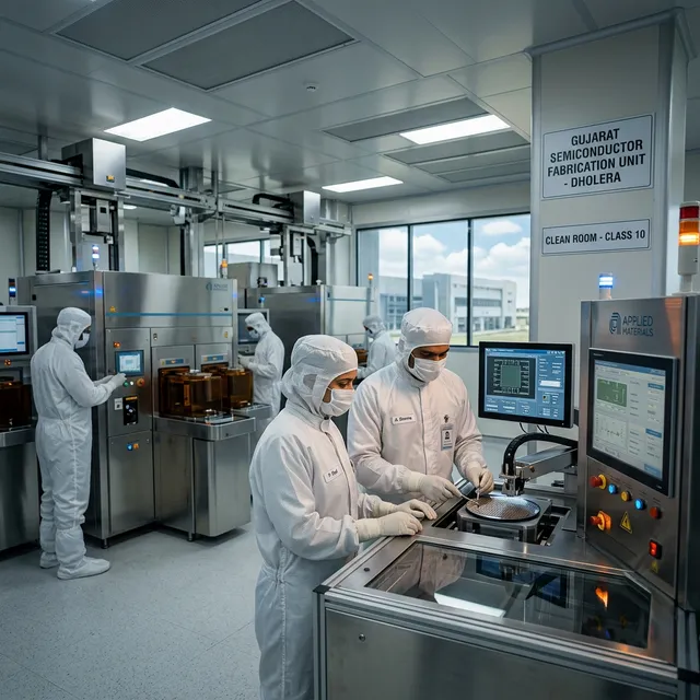
Tata Electronics + PSMC (Taiwan) Fab in Dholera, Gujarat: This is the flagship project of the India Semiconductor Mission and the most ambitious. Tata Electronics, in partnership with Taiwan's Powerchip Semiconductor Manufacturing Corporation, is constructing a semiconductor fabrication facility in the Dholera Special Investment Region. The facility will manufacture chips at the 28nm process node—which requires immediate, important context to understand properly.
The 28nm node is not cutting-edge. Taiwan's TSMC currently manufactures chips at the 3nm node; Samsung is producing at 3nm; Intel is ramping 18A (roughly 1.8nm equivalent). The 28nm node is approximately four to five generations behind the current frontier. This gap may sound embarrassing, but it is not. It is, in fact, the most strategically intelligent starting point available. The 28nm node is what the semiconductor industry calls a "sweet spot"—mature enough that the manufacturing processes are well-characterized and the equipment is available, yet advanced enough to serve enormous, high-volume markets. Approximately 30-35% of all semiconductors manufactured globally are produced at the 28nm node or above. These chips power automotive electronic control units, industrial automation systems, IoT devices, power management circuits, display controllers, Wi-Fi modules, and the vast infrastructure of modern electronic devices that do not require cutting-edge transistor density but absolutely require reliable, high-volume supply.
Micron Technology's ATMP Facility in Sanand, Gujarat: Micron—one of the world's three major memory semiconductor manufacturers—is building an Assembly, Test, Marking, and Packaging (ATMP) facility with a $2.75 billion investment. This facility will not manufacture chips from raw silicon; instead, it handles the critical back-end processes of taking manufactured semiconductor dies (from fabs elsewhere), packaging them into usable integrated circuit components, testing their functionality, and preparing them for integration into electronic products. This is not glamorous, but it is extraordinarily important—packaging technology is increasingly becoming a major source of performance innovation, and India's entry into this segment of the supply chain builds genuine manufacturing competence.
CG Power and Renesas Joint Venture: Another back-end facility focused on chip packaging and testing, further reinforcing India's strategy of establishing credibility in semiconductor manufacturing through the more accessible back-end processes before attempting the far more complex front-end wafer fabrication.
The Brutal Engineering Realities
Infrastructure at Unprecedented Standards: A semiconductor fab's infrastructure requirements are not merely stringent; they are unlike any other industrial facility on Earth. The Dholera facility will require massive quantities of ultrapure water—semiconductor-grade water with fewer than five parts per billion of dissolved minerals—delivered continuously, without interruption, 24 hours a day, 365 days a year. It will require completely uninterruptible power supply; not "99.9% reliable" power, but literally zero unplanned outages, because a single power fluctuation measured in milliseconds can destroy an entire production batch. India's industrial power infrastructure, while dramatically improving, does not yet deliver this level of reliability uniformly, and the Dholera facility is being constructed with dedicated power infrastructure to guarantee these standards.
The Talent Transformation Challenge: India possesses world-class semiconductor design talent—this is documented, demonstrated, and globally acknowledged. What India almost entirely lacks is semiconductor manufacturing talent: the process engineers, equipment technicians, yield optimization specialists, contamination control experts, and fab management professionals who understand how to operate a fabrication facility at the extraordinary precision standards required. This talent deficit is not a matter of intelligence; it is a matter of experience, and experience can only be developed by operating actual manufacturing facilities. Training programs are underway—collaborations with TSMC, partnerships with international semiconductor equipment companies, dedicated academic programs at IITs—but building a workforce capable of operating a world-class fab takes five to seven years of intensive, hands-on experience accumulation.
The Supply Chain Ecosystem: A semiconductor fab does not operate in isolation; it depends on an extensive ecosystem of specialized suppliers: ultra-high-purity chemical providers, precision gas delivery systems, photomask manufacturers, cleanroom equipment specialists, wafer handling automation systems, and metrology instrument companies. This ecosystem currently exists in Taiwan, South Korea, Japan, and parts of the United States and Europe. Building an equivalent ecosystem in India—or establishing reliable international supply chains to serve Indian fabs—is a massive, multi-year undertaking that requires dozens of specialized companies to establish Indian operations simultaneously.
The Strategic Calculus: Why India Cannot Afford Not to Try
The COVID-era global chip shortage—which paralyzed automobile production, delayed consumer electronics launches, and exposed the terrifying fragility of global semiconductor supply chains—demonstrated with brutal clarity why semiconductor manufacturing is a national security imperative. India imports approximately $10 billion worth of semiconductors annually. Every chip in every defence system, every telecommunications network, every power grid controller, every medical device is manufactured in a foreign country and transported across oceans before reaching Indian soil. In a geopolitical crisis—a Taiwan Strait confrontation, a trade war, even a natural disaster disrupting shipping routes—India's access to the silicon that powers its entire modern infrastructure could be disrupted overnight.
The India Semiconductor Mission is, at its core, a strategic diversification program. Even partial success—domestically manufacturing 20-30% of the mature-node chips that India currently imports entirely, while continuing to source cutting-edge processors internationally—would dramatically improve supply chain resilience, reduce the trade deficit, and create a foundation of manufacturing expertise that can be progressively advanced over decades.
Frequently Asked Questions (FAQs)
Why can't India just start manufacturing at the cutting-edge 3nm node like TSMC?
Because cutting-edge semiconductor manufacturing is the product of cumulative, sequential learning that cannot be skipped. TSMC did not suddenly produce 3nm chips; it spent 35 years progressing through every preceding node—250nm, 180nm, 130nm, 90nm, 65nm, 40nm, 28nm, 16nm, 7nm, 5nm—accumulating process knowledge, yield optimization expertise, and equipment mastery at each stage. Each node transition required solving novel physics and engineering challenges that could only be understood by mastering the previous generation. No country or company in history has successfully leapfrogged multiple manufacturing nodes. India must start where the learning begins, and 28nm is that rational, proven starting point.
Is $10 billion enough to build a semiconductor manufacturing ecosystem?
It is enough to begin. A single cutting-edge fab (3nm or below) costs $15-20 billion to construct. India is not building a cutting-edge fab; it is building mature-node facilities where construction costs are $5-8 billion per fab. The $10 billion budget covers initial fab construction, ATMP facilities, design ecosystem support, and training infrastructure. If the mission succeeds at this scale, significantly larger investments—both government and private—will follow. TSMC alone has invested over $100 billion in manufacturing capacity over its lifetime. India's initial $10 billion should be understood as a strategic down payment, not a total budget.
Will Made-in-India chips be competitive with chips from Taiwan or South Korea?
At mature nodes (28nm and above), competitiveness is primarily determined by yield rates (the percentage of manufactured chips that pass quality testing), cost efficiency, and reliability—not by frontier technology innovation. Indian fabs will initially have lower yields than established Taiwanese or Korean facilities, resulting in higher per-chip costs. This disadvantage narrows over time as manufacturing teams accumulate experience and optimize processes. For certain applications—particularly defence, automotive, and critical infrastructure where supply chain sovereignty is more important than absolute cost minimization—Made-in-India chips will be competitive from day one because their value proposition includes strategic independence, not just unit economics.


Comments (0)
Be the first to share your thoughts on this article.